Firing feature-driven neural circuits with scalable memristive neurons for robotic obstacle avoidance

Biological background
Invertebrates often rely on a simple neural circuit consisting of several neurons to control their activities14. In these circuits, sensory interneurons are considered to be detectors of predator signals, with functions that activate the descending neuron and dominate the avoidance behavior of organisms to the approaching danger30,31,32,33. Figure 1A shows the neural circuits of crickets that conduct such avoidance behavior, which consists of auditory receptors, auditory interneurons, and descending motor neurons. The auditory receptors receive ultrasonic information at cricket ears located on the tibiae of the forelegs and generate action potentials34,35. Then, the generated action potentials are transmitted to the auditory interneurons (named AN2) located at the prothoracic ganglion and are encoded as spiking features to transmit to the descending neurons36,37. Next, two descending neurons decode the received signals and generate specific spiking features to control the avoidance behavior of the crickets38,39. Biologists have found that, except for the spiking feature, AN2 neurons also prompt the high frequency bursting feature that dominates the avoidance behavior of crickets under the ultrasonic stimulus, exhibiting a mixed firing behavior40. The descending neurons decode the “bursting” and “spiking” features in the mixed pattern via a selective communication scheme, which includes an asynchronous decoding function and ensures a timely response. In addition, the properties of bursting—high frequency41, high reliability42, and strong stimulation to postsynaptic neurons43—are advantageous when signals are required to trigger responses very quickly. This behavior allows the sensory system to make early decisions to take evasive actions, facilitating reliable and rapid responses. These principles demonstrate the intelligence of insects, which inspires our avoidance system design.
A Schematic of the biological neural circuit associated with escape behavior in crickets. Ultrasonic signals are received by the receptors, transmitted to AN2 neurons for encoding and then decoded by the descending neurons to control the behavior of crickets. The high-frequency “bursting” feature of AN2 neurons causes crickets to escape. B Schematic of the neuro-inspired SCNC. The distance information from the obstacle is transmitted to the ascending memristive H-H neuron (mixed-coded neuron, MCN) through LiDAR, encoded as spiking features, and then decoded by two descending memristive H-H neurons (bursting detection neuron, BDN and spiking detection neuron, SDN) to control the steering and actuating of the robot, respectively. C Obstacle avoidance scheme related to the robot-obstacle distance. The steering angle and moving speed are controlled by the firing frequencies of BDN and SDN, respectively.
Inspired by the cricket’s avoidance neural circuits, we develop an SCNC comprising a LiDAR sensor and three H-H neurons based on NbO2 memristors to support the robot in performing obstacle avoidance (Fig. 1B). The LiDAR sensor emulates the auditory receptor and encodes the robot-obstacle distance into voltage signals. One H-H neuron serves as the AN2 interneuron to receive the input from the sensor and encode the distance-related voltage into mixed firing patterns, named mixed-coded neurons (MCN). A key point is that the H-H interneuron features a probabilistic transition from spiking to bursting, and the bursting ratio increases as the input intensity increases, which is attributed to the intrinsic stochasticity of memristors. The other two NbO2 H-H neurons emulate the descending neurons that extract the bursting and spiking features from the encoded mixed pattern in the interneuron. This operation reliably emulates the selective communication scheme observed in biology. According to the functions, we denoted these two neurons bursting-detection neuron (BDN) and spiking-detection neuron (SDN). Then, we utilize the firing frequency of BDN and SDN to control the steering motors and actuating motors, respectively. The firing frequency of the BDN increases as the distance-related voltages increase, while the SDN is vice versa. Thus, the closer the obstacle is to the robot, the larger the steering angle and the slower the speed, as shown in Fig. 1C. Then, the obstacle avoidance response of the robot is achieved by equipping it with such an SCNC and computing with firing features.
H-H neurons based on NbO2 memristors
We build our SCNC inspired by the circuit structure in ref. 26. We first construct an H-H neuron using NbO2 memristors, as shown in Fig. 2A. The H-H neuron circuit comprises two resistors (R1, R2), two capacitors (C1, C2), and two NbO2-based threshold switching (TS) memristors with d.c.-biased provided by two voltage sources (E1, E2). These two TS devices represent the sodium and potassium ion channels in biological neurons, respectively. The device is configured with a Pt/NbO2/Ti structure (see more fabrication details in Supplementary Fig. 1 and Methods). To demonstrate H-H neuron circuits, we connect the TS devices fabricated in the laboratory with off-the-shelf resistors and capacitors via a printed circuit board (PCB) in this work. Figure 2B shows the typical I-V curve of the two NbO2 TS memristors and the built model (see Methods for device models). The two devices show nearly identical electrical performance, reducing the difficulty of setting the H-H circuit parameters. Initially, the device is in a high resistance state (HRS). When the voltage applied to the top titanium electrode surpasses the threshold voltage (VTH), the device switches from HRS to a low resistance state (LRS) under a 400 μA compliance current. Once the applied voltage is less than the hold voltage (VHold), the device spontaneously switches back to the HRS. Due to the electron-related switching mechanism, the device exhibits a fast switching speed (~1 ns)22 and high endurance (>1010 cycles)23, which is decent for neuronal applications. According to the spike numbers within one cluster, the spiking and bursting features are two basic features that enable the neurons’ various firing behaviors. Thus, we illustrate the mechanisms of the generation of spiking and bursting action potentials through simulation, as shown in Fig. 2C. The top panel illustrates both TS devices’ switching sequence and the dynamic output action potentials when the circuit behaves in a spiking feature. In this case, TS2’s switching-on time is behind TS1’s switching-off (see more detailed description of the switching procedures in Supplementary Fig. 2). When the circuit parameters change, TS2 may switch on before TS1 switches off. Under these circumstances, the voltage of the positive constant voltage source E2 charges C1 through the coupled R2, resulting in a delay in the switching off of TS1 normally, which results in twice switching on/off of TS2 and then completing a bursting fire (see more details in Supplementary Fig. 3). Thus, the output pattern of the neuron circuit can be controlled by adjusting the circuit parameters to regulate the relative switching time between two TS devices. Changing the two capacitors’ capacitances to control the firing features of the output in other literature29 follows this principle. In addition, neuron circuits used for neuromorphic computing usually receive both positive and negative inputs. The H-H neuron circuit we construct is also capable of accepting negative inputs and the integration of both positive and negative inputs (see more details in Supplementary Fig. 4). Based on such an H-H neuron circuit with NbO2 memristors, we successfully demonstrated 23 natural firing behaviors (see Supplementary Fig. 5 and Supplementary Table 2), as reported in other literatures26,44.
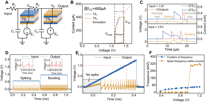
A The H-H neuron consists of two resistors (R1, R2), two capacitors (C1, C2), and two TS devices (TS1, TS2) with opposite bias voltages provided by two voltage sources (E1, E2). B Typical volatile threshold switching behavior of two TS devices used in the H-H neurons. Both TS devices exhibit similar VTH and VHold. C Top panel: Schematic of TS devices’ switching sequence and dynamic output action potentials when the circuit behaves in a spiking feature, in which TS2’s switching-on time is behind TS1’s switching-off. Bottom panel: Schematic of TS devices’ switching sequence and the dynamic output action potentials when the circuit behaves in a bursting feature, in which TS2’s switching-on time is before TS1’s switching-off and TS2 switches twice. (Simulation) D The neuron output presents two different firing features under different input voltages. When the input is 0.7 V, the neuron fires in the spiking feature, showing regular single-spike output, and when the input is 1.2 V, the neuron fires in the bursting feature with two spikes per burst. (Experiment) E Under triangle wave scanning with an amplitude of 1.3 V, the output of the neuron shows a transition between the two firing features. When the input is ~1.0 V, the output of the neuron transitions from spiking to bursting. (Experiment) F Neuronal output frequency as a function of input voltage. The firing cluster frequency of the neuron increases linearly with increasing voltage. When the voltage input is 1.0 V, bursting starts to appear in the neuron output, corresponding to a large bursting spike frequency. (Experiment).
For emulating AN2 neurons, the spiking and bursting features should emanate from a fixed neuron. Thus, according to the studied mechanisms, we carefully set the circuit parameters such that the switching-off time of TS1 and the switching-on time of TS2 is close at a lower input. Under such parameters, when the input increases, the switching-off time of TS1 and the switching-on time of TS2 gradually approach each other, that is, the time difference ∆t between them gradually decreases until TS2 switches on before the switching off of TS1, which in turn prevents the switching off of TS1, completing the transition from spiking to bursting. Thus, we achieve both “spiking” and “bursting” features in a fixed circuit through simulation (Supplementary Fig. 6, parameters are shown in Supplementary Table 3). Then, based on the simulation parameters, we conduct an experiment on the NbO2-based H-H neuron, as shown in Fig. 2D. Under a low constant input voltage (0.7 V), the neuron fires in the spiking feature (fires in a single peak), while the neuron fires in the bursting feature (fires in two peaks per cluster) when the applied voltage increases to 1.2 V. The results show that through carefully modulating the parameters, our neuron circuit successfully emulates the behavior of AN2 neurons. To further illustrate that the transition between spiking and bursting features is continuous and reversible (Fig. 2E), we applied a triangular pulse with an amplitude of 1.3 V as the input of the neuron circuit. At very low voltages (<~0.3 V), the neuron fires no spike. When the input gradually increases, the neuron begins to fire in spiking feature, and the interspike intervals gradually decrease with increasing the input voltage, signifying that the neuron’s output frequency gradually increases. As the voltage continues to increase (up to ~1.0 V), the neuron transitions to fire in bursting feature, and the intervals between bursts gradually decrease. When the amplitude of the triangular input is 0.9 V and 2.2 V (Supplementary Fig. 7), the output continues to satisfy the above requirements, which indicates a reversible firing feature transition behavior. To more clearly present the firing feature transition under different input voltages, we analyze the firing frequency evolution, as shown in Fig. 2F. We define every firing event between two adjacent refractory periods as a cluster, regardless of whether there are single or two peaks (spikes or bursts) in one cluster. The cluster frequency increases almost linearly with increasing the input voltage, consisting of the effect of the input intensity on frequency in the spiking feature only (blue line). In addition, the firing frequency within a burst is particularly high when the bursting feature starts to appear in the firing pattern of the output, even up to 320 kHz, which also increases with increasing input voltage (yellow line). The characteristic of the high frequency of bursts makes it easy to distinguish them from the spikes in the spiking feature. The results show that our H-H neuron with intensity-driven feature transition behavior has the potential to be used for encoding emergencies, similar to the AN2 neuron.
Probabilistic feature transition in NbO2-based H-H neurons
In biological AN2 neurons, the transition between spiking and bursting features is not a binary event14. Rather, the firing patterns mix both features, in which the ratio of the bursting feature is related to the stimuli intensity and the stochasticity of ions moving through the channels. These characteristics provide the AN2 neuron with powerful encoding capability. To emulate the mixed firing pattern with both features of the AN2 neurons, we further studied to endow the intrinsic stochastic switching of TS devices into the feature transition processes. This occurs because the randomness of VTH, VHold and the resistance of the two devices affects the relative switching on or off timing of these two TS devices and hence may result in a probability transition behavior with mixed spiking and bursting rather than an abrupt transition. First, we explore the effect of the randomness of the VTH and VHold on the output. Figure 3A shows 50 DC switching cycles of the two TS devices used under a 400 µA current. Clearly, the VTH and VHold values of both devices fluctuate, which is helpful for enabling mixed firing features because the firing feature is affected by the relative switching on or off timing of these two TS devices. To further demonstrate that the switching cycle is stochastic, we extracted the VTH and VHold values of both devices in 5000 cycles from an oscillator circuit in Supplementary Fig. 8. The results confirm that the distribution of VTH and VHold of the two devices is highly uniform and satisfies a Gaussian distribution (Fig. 3B and Supplementary Fig. 9), proving the randomness of the devices and thus has great potential to enable the probabilistic transition of H-H neurons. According to the previous analysis, the voltage values of the two sources are redesigned to reside between \(\frac{{V}_{{TH}}+{V}_{{Hold}}}{2}\) and VTH, enabling the H-H neuron to work in a probabilistic transition state. We first study how the devices’ stochasticity affects the output firing features through simulation. Figure 3C shows the output phase diagram of the neuron circuit when the variation is within a range satisfying the Gaussian distribution in Fig. 3B. When both TS1’s VHold and TS2’s VTH are at the mean value, the neuron’s output is in the critical state of the transition from spiking to bursting feature. When both TS1’s VHold and TS2’s VTH decrease, the switching-off time of TS1 is delayed and the switching-on time of TS2 is advanced, which results in a pure bursting feature. Conversely, when both TS1’s VHold and TS2’s VTH increase, the switching-off time of TS1 is advanced, and the switching-on time of TS2 is delayed. The output of the neuron circuit fires in a pure spiking feature. When the VHold of TS1 and the VTH of TS2 change in opposite trends, the feature of the circuit’s output is uncertain. Therefore, when the VTH and VHold of the devices vary within a certain range, the circuit generates mixed firing features under a constant input. We note that instead of TS1’s VHold and TS2’s VTH, TS1’s VTH and TS2’s VHold also affect the firing features, which we do not discuss here one by one individually. Similarly, we also explore the effect of the high and low resistance randomness of the device on the circuit output, as shown in Supplementary Fig. 10. It is shown that the combination of the randomness of VTH, VHold, the high and low resistance value of the two devices results in the probabilistic transition behavior of the circuit output. Figure 3D shows the neuron’s firing output under three different input intensities in the experiment. Under a low input voltage (0.9 V), the neuron fires with a pure spiking feature (top panel). When increasing the input voltage to 1.2 V, the neuron’s output contains both spiking and bursting features, showing probabilistic transition behavior (middle panel). When the input voltage is sufficiently high, the neuron fires with a pure bursting feature (bottom panel). The results show that after careful design, our neuron successfully emulates the mixed transition behavior in AN2 neurons.
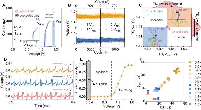
A The switching cycles of the two TS devices used for the H-H circuit, showing similar VTH and VHold with random fluctuations. B The VTH and VHold of the two devices show some randomness under 5000 cycles and satisfy the Gaussian distribution. C The output phase diagram of the neuron circuit when the VHold of TS1 and the VTH of TS2 vary within a range satisfying the Gaussian distribution. When the VTH and VHold of the devices are randomly changed in a certain range, the circuit can generate mixed firing features under constant input. The voltage values of the two sources are designed to be within \(\frac{{V}_{{TH}}+{V}_{{Hold}}}{2}\) and \({V}_{{TH}}\). (Simulation) D The output of the neuron shows probabilistic transition behavior under different voltage inputs. At 0.9 V, the output of the neuron is in the spiking feature. At 1.2 V, the output of the neuron presents a mixed pattern of bursting and spiking, and at 1.5 V, the output is in the bursting feature. (Experiment) E The bursting probability of the neuron increases with the input voltage. (Experiment) F Joint interspike interval (JISI) scatter plots of the spike train with input from 0.3 V–1.5 V. (Experiment).
Figure 3E shows the calculation of the bursting probability of the neuron circuit under input voltage pulses (0.3 V–1.5 V, 500 µs) with a step of 0.1 V according to the data from Fig. 3D and Supplementary Fig. 11. To explore how the input intensity affects the feature transition processes, we define bursting probability as the ratio of bursting numbers to all cluster numbers during pulse application. When the voltage is low (<1.0 V), there is no burst in the output, which entirely comprises spiking, such the bursting probability is zero. When the input voltage increases to 1.0 V, some spikes transition to the bursts. With further increasing input, the bursting probability increases. When the input intensity is high enough, the influence of the input voltage increase exceeds the stochasticity induced by the TS devices, and the neuron fires continually in the bursting feature. To observe the properties of the firing pattern of the output under different inputs, we plot the interspike interval-time curve (see Supplementary Fig. 12). The results show that the interspike interval time exhibits irregular oscillations when the neuron fires in a mixed pattern, while it shows a constant or regular oscillation curve under a pure spiking or bursting case. To clearly illustrate the characteristics of the two firing features, the Joint Interspike Interval (JISI) scatter plots, which are also named interval return maps, of the spike trains are presented. The JISI plot is a classical stochastic spike train analysis method used to explore the relationship between adjacent ISIs45,46,47. We defined ISIi = tn − tn-1, where tn is the time of the nth spike (see Supplementary Fig. 13). By plotting the statistical distribution of adjacent ISIs, we could obtain the JISI plot and establish the serial correlation of adjacent points in the time series, which is helpful to judge and predict the firing pattern. Figure 3F shows the plotted JISI scatter plot of the neuron circuits under different input intensities. When the input is <1.0 V, the neuron fires in a pure spiking feature (yellow points), and the ISI points are gathered in the diagonal position, indicating that the interval between spikes is basically unchanged. When the input is no less than 1.5 V, the neuron fires with a pure bursting feature and the ISI points are distributed along the coordinate axis (pink points). The ISIs of the first spikes in the bursts are closer to the X axis, while the ISIs of the second spikes are closer to the Y axis. When 1.0 V < input < 1.5 V, the neuron fires in a mixed pattern, and ISIs are located partly on the diagonal and partly in the region close to the coordinate axis (blue points). Thus, through the distribution of ISIs, we effectively distinguish whether bursting features are included in the output for different input intensities. These results demonstrate that the intrinsic stochasticity of the device enhances the encoding capability of H-H neurons and is a powerful source to enable feature-driven computing.
Selective communication scheme in H-H neurons
To result in the execution of functional responses, the mixed firing features generated by the AN2 neurons need to be further decoded by the descending neurons that control related motor neurons. Biologists have found that there is a selective communication mechanism between biological neurons, attributed to the subthreshold oscillation characteristics of biological neurons48,49. The descending neurons generate action potentials only when the input frequency matches their subthreshold oscillation frequency (see Supplementary Fig. 14 for more details). That is, descending neurons respond to those inputs with specific resonant frequencies. Specifically, neuron A sends spike trains with mixed firing features to neurons B and C, which have different subthreshold resonant frequencies, as shown in Fig. 4A. Neuron B, with a higher subthreshold oscillation frequency, resonates with the bursting feature at the higher frequency generated by neuron A and then generates action potentials but does not respond to the spiking feature. Neuron C, with a lower subthreshold oscillation frequency, responds with the opposite behavior. Consequently, descending neurons B and C can selectively respond to specific information in a mixed pattern from ascending neurons, which demonstrates intriguing inherent cognitive capabilities.
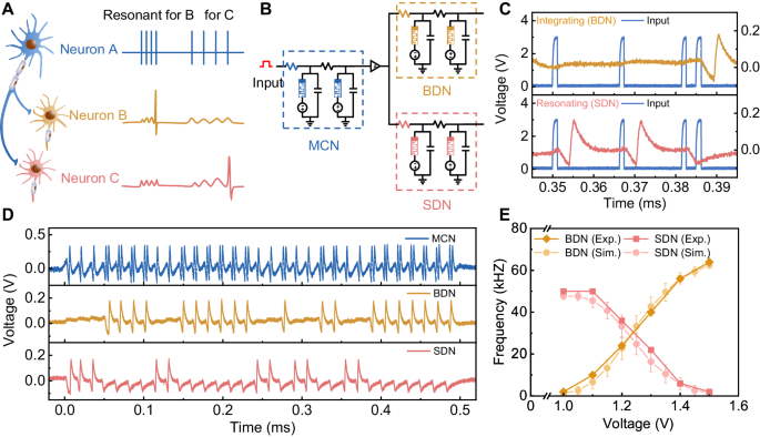
A Schematic of selective communication of biological neurons. Postsynaptic neurons selectively transmit information from presynaptic neurons by responding to specific firing features with a resonance behavior. B Schematic of an artificial neural circuit emulating the biological selective communication circuit. The three memristive H-H neurons are configured with different circuit parameters. C The selective communication scheme in the memristive neural circuit. The resonance characteristic of the BDN neuron enables it to produce spike responses only to inputs with low frequency but not to inputs with high frequency. The integration property, on the other hand, makes the SDN neuron capable of producing spike output only for inputs with a high frequency. D The selective communication scheme of the neural circuit under continuous inputs. The SDN neuron with resonance characteristics can extract single spikes from the output of the mixed pattern of the MCN and generate spike responses, and the BDN neuron with integration characteristics extract bursts from the output of the MCN. E The firing frequencies of SDN and BDN under different input voltages on the MCN neuron. The simulation data is well-fitted with the experimental results. The error bars represent the standard deviation (σ) of each group.
Inspired by the selective communication scheme between biological neurons, we configure another two NbO2-based H-H neurons with different circuit parameters (see Supplementary Table 3) to process the mixed pattern sent by the AN2-like H-H neuron. These two neurons are denoted BDN and SDN according to their functions. The neural circuits built upon these three neurons are intended to emulate the crickets escape neural circuit, as shown in Fig. 4B. The MCN encodes the input stimuli intensity, generating a mixed pattern that contains both spiking and bursting features, as discussed. The BDN fires action potentials after bursts from the MCN are detected, while the SDN neuron detects the spikes in the spiking feature. To improve the fan-out ability of the MCN, we adopted a comparator as the interface to transmit signals to the following descending neurons. Here, it should be noted that we design these three neurons under the same structure, which lowers the complexity of system design and enables us to build flexible systems when the neuron’s components are configurable. Figure 4C shows the firing behaviors of the BDN and SDN under identical inputs with a mixed pattern. The BDN generates an action potential when the input is at a high frequency but does not respond to the low-frequency input (top panel of Fig. 4C), serving as an integrator26,44. While the SDN only responds to the low-frequency input (bottom panel of Fig. 4C), serving as a resonator44,48. These results show that the designed BDN and SDN could successfully detect bursting and spiking features, respectively.
To further demonstrate the selective communication function of the constructed neural circuit, we applied a 1.3 V voltage with a 500 µs duration on the AN2-like H-H neuron and tested the output of the two descending neurons. The firing behaviors of these three neurons are shown in Fig. 4D. When the stimuli input is applied, the MCN fires with a mixed pattern due to the probabilistic transition (top panel). Under this condition, such a mixed spike train is transmitted to both the BDN and SDN. The BDN fires only when a bursting event occurs (bottom panel), while the SDN only responds to the spiking event (bottom panel). We also tested the output of the neural circuits under different input voltages, emulating the response of the neural circuit under different stimulus intensities, as shown in Supplementary Fig. 15. The higher the input voltage is, the higher the probability of bursting features, resulting in a higher fire frequency of the BDN and a lower frequency of the SDN. To more clearly present the computing process of the neural circuit, we plotted the average frequency output of BDN and SDN under different input voltages (the solid lines in Fig. 4E). To further illustrate the validity of the relationship between the input voltage and bursting/spiking firing frequency, we construct a mathematical device model with stochasticity of switching voltages and introduce it in the H-H neuron circuit. The simulated data is well matched with the experimental data, as shown in Fig. 4E (see more details in Supplementary Text 1 and Supplementary Fig. 16). Under an input voltage <1.0 V, the BDN neuron fires no spikes, indicating that there are no accidental triggers. When the input voltage increases to 1.0 V, the BDN starts to fire and the firing frequency increases as the input intensity increases, corresponding to the increased bursting probability. The SDN’s output behaves vice versa. When the input voltage is high enough, the BDN exhibits the highest frequency, while the SDN fires no spikes. These results show that the constructed neural circuit could successfully encode stimuli with mixed firing features and decode them through the intrinsic selective communication properties of neurons, faithfully emulating the functions of cricket escape neural circuits.
Robot obstacle avoidance system with constructed SCNC
Mobile robots need to complete tasks intelligently in complex and changeable environments in a real-time and low-power manner50. When encountering an abrupt danger, such as an incoming high-speed obstacle, the robot needs to react as quickly as possible to ensure its safety. Inspired by the reflex-like self-protection behavior of crickets for dodging predators, we present a strategy by equipping the SCNC on a robot to enable obstacle avoidance behavior in an emergency and achieve a rapid response. Our workflow is shown in Fig. 5A. LiDAR serves as the sensor, detecting obstacle distances. These distances are translated to voltages that serve as the input of the SCNC. The voltage is defined as inversely proportional to the distance. The MCN encodes the input voltage into mixed patterns. The SDN detects the spikes from the MCN, and the firing output is used to drive the actuating motors. Meanwhile, the BDN detects the bursts from the MCN, and the output is utilized to control the steering motors. The BDN and SDN output frequencies are positively proportional to the angular velocity and linear velocity, respectively. The right part of Fig. 5A depicts three typical cases during driving. When the obstacle is quite far away, the MCN is driven by low voltage input to generate spike trains with pure spiking features, and thus, the SDN has the highest frequency output. In this case, the robot is actuated with the highest speed and moves straight (top panel). When an obstacle is relatively close, the input voltage enables the MCN to fire with mixed firing features, and the BDN neuron starts to fire to drive the steering motors. The robot decelerates and turns at a small angle (middle panel). When a sudden obstacle is very close, the robot executes an emergency response, namely, braking and rapid turning at a large angle, to remove the obstacle to a safe zone and prepare for the next straight move (bottom panel).
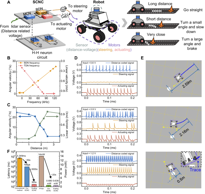
A Schematic diagram of the robot avoiding an obstacle that appears at different distances. B The angular and linear velocities are linearly proportional to the BDN frequency and SDN frequency, respectively. A reasonable maximum linear velocity (0.9776 m/s) is set here. C An illustration of the relationship between variable distance range and the responses determined by SCNC, involving angular velocity and linear velocity. D The firing patterns of the MCN (blue), BDN (yellow) and SDN (red) are associated with the ‘distance coded’ signal, ‘steering’ signal and ‘actuating’ signal, respectively. E The indoor trajectory recording of a robot vehicle under three typical features. The motion trace is in the cyan line, and the steering angle is in yellow. F Comparison of time latency between the obstacle avoidance scheme implemented by conventional methods (NVIDIA Jetson AGX Xavier), our physical SCNC and the SCNC after scaling. And a comparison of power consumption between the obstacle avoidance scheme implemented by FPGA, our physical SCNC and the SCNC after scaling.
The linear mapping relationship between the firing frequency of BDN (SDN) and the angular velocity (linear velocity) during the experiment is shown in Fig. 5B. Figure 5C shows the angular velocity and linear velocity output of the robot at different distances. The closer the robot is to the obstacle, the smaller the linear velocity and the larger the angular velocity. Figure 5D shows the output results of the SCNC under three different distances. The distance information detected by the LiDAR is encoded as an input voltage and transmitted to the SCNC. The MCN, BDN and SDN in the circuit generate corresponding firing behaviors, which represent the “distance coded” signal, “steering” signal, and “actuating” signal, respectively, and are transmitted back to control the robot. The movement trajectory of the robot in the physical environment is recorded during the experiment to represent the linear velocity (length of the cyan trajectory) and angular velocity (angle marked by the yellow line) of the robot while driving. When the obstacle is quite far away (2.59 m), the decoded actuating signal has a high frequency response (top panel of Fig. 5D). In this case, the linear velocity reaches the maximum (0.9776 m/s), while the angular velocity is negligible because the steering signal contains few spikes. Therefore, the robot is quite safe and thus moves straight quickly (top panel of Fig. 5E). Once the obstacle appears within a preset dangerous distance range (2.16 m), the MCN fires in a mixed pattern (middle panel of Fig. 5D), representing certain danger is detected, and the steering signal and the actuating signal are used to drive obstacle dodging. The robot navigates around the obstacle with a moderate speed and angular velocity (middle panel of Fig. 5E). In contrast, if the robot notices that an abrupt incident occurs in close proximity (0.5 m) and does not have enough time and space for reaction, it rapidly decelerates and makes a sharp turn to ensure safety. Under such a circumstance, the distance coded signal exhibits almost all bursting (bottom panel of Fig. 5D), which gives rise to maximum angular velocity and minimum speed (bottom panel of Fig. 5E). Actually, these three responses in Fig. 5d, e are just discrete slices of continuous motion. In a continuous emergency response process, these movements are combined at different time durations to accomplish a complete obstacle avoidance course. More experimental details are presented in Methods and Supplementary Figs. 17–19. Supplementary Movies 1–4 show the whole emergent obstacle avoidance process.
Moreover, we calculate the average latency executed by the traditional CMOS computing unit in the NVIDIA Jetson AGX Xavier and compare it to that of our SCNC. After 500 trails of recording, the data shows that our SCNC alleviates the delay burden of robotic movement. It should be noted that the latency considered here is between receiving the distance signal and publishing the motion command. During the measurement, we processed the distance information as a voltage input with a pulse width of 200 μs, in which case the latency of the circuit is 200 μs. Here, we define the minimum inference time during which the statistical firing rate curve still obeys the relationship in Fig. 4E, as the minimum delay. When the pulse width is reduced to 100 μs, the statistical curve is still decent (see Supplementary Fig. 20). Therefore, we consider the minimum delay of the circuit to be 100 μs under the current circuit parameters. Figure 5F illustrates the statistical results, and the latency of leveraging physical SCNC to directly drive the robot behavior is reduced by ~50 times. In fact, the minimum delay of the circuit is mainly determined by the two capacitors C1 and C2 in the circuit. When the capacitance of the device is reduced to an ~fF level (C1 = 500 fF, C2 = 100 fF of MCN)22, the minimum delay of the circuit can be reduced to 30 ns (see Supplementary Fig. 20). At the same time, we conducted an evaluation of our obstacle avoidance approach on a Xilinx XCZU2CG-1SFVC784E (operating at a frequency of 25 MHz with a 1.8 V I/O standard), comparing its power consumption with our NbO2 SCNC hardware realization scheme. The results show that the highest average power consumption of three H-H neurons in the SCNC is 0.680 mW, while the FPGA consumes an average of 14 mW, indicating that the power consumption of our NbO2 SCNC is <5% of FPGA. The power consumption of the SCNC could be as low as ~0.636 mW when the capacitances are scaled, which achieves largely lower total energy consumption attributed to the smaller latency. In this case, each spike’s energy consumption of the circuit can also be reduced to 1.06 pJ/Spike (see Supplementary Fig. 21 and Supplementary Table 4). These results indicate the great potential of our SCNC for the application of mobile intelligent robot emergent obstacle avoidance.


